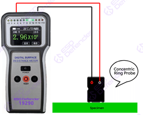
Introduction to Resistivity Testing in Electronics
Resistivity testing serves as a critical quality gate for electronic materials, ensuring consistent electrical performance across manufacturing processes. As device geometries shrink and material requirements tighten, precise resistivity measurement has become indispensable for semiconductor wafers, conductive films, and dielectric substrates. This article examines how resistivity verification safeguards product quality throughout the electronics supply chain.
Table of Contents
Fundamentals of Material Resistivity
Resistivity (ρ) quantifies a material’s inherent opposition to current flow, measured in ohm-meters (Ω·m). In electronic materials, this property directly impacts:
– Charge carrier mobility in semiconductors
– Signal loss in interconnects
– Thermal management efficiency
– ESD protection performance
Key Applications in Semiconductor Manufacturing
Wafer Doping Verification
Four-point probe resistivity measurements:
– Validate dopant concentration uniformity
– Detect diffusion process variations
– Identify crystal defects in silicon ingots
– Comply with SEMI MF84 standards
Thin Film Characterization
Resistivity mapping reveals:
– Deposition uniformity across substrates
– Anisotropy in transparent conductive oxides
– Thickness variations in metal layers
– Process drift in sputtering systems
Printed Circuit Board Material Evaluation
Substrate Quality Control
Impedance testing ensures:
– Proper dielectric constant in FR-4 laminates
– Consistent copper foil conductivity
– Absence of delamination or voids
– Compliance with IPC-4101 specifications
Conductive Ink Performance
Resistivity testing verifies:
– Nanoparticle dispersion quality
– Curing process effectiveness
– Adhesion reliability
– Batch-to-batch consistency
Advanced Packaging Material Assessment
Interconnect Reliability
Resistivity monitoring detects:
– Kirkendall void formation
– Intermetallic compound growth
– Electromigration onset
– Thermal cycling damage
Thermal Interface Materials
Testing confirms:
– Filler particle distribution
– Proper curing of polymer matrices
– Stable performance under load
– Degradation thresholds
Measurement Method Selection Guide
When working with materials that require precise electrostatic control, choosing the correct measurement method is critical to ensure both accuracy and efficiency. The method must match the material type, application environment, and production speed. Here’s a breakdown of common measurement techniques and where they best apply:
Four-Point Probe Technique
This is widely regarded as the gold standard in the microelectronics and semiconductor industries, particularly for wafers and thin films:
- Eliminates contact resistance errors: By using separate current-supplying and voltage-sensing probes, this technique avoids skewed results caused by contact resistance.
- Highly accurate for sheet resistance: Particularly effective for uniform films and coatings used in microchip fabrication.
- Ideal for R&D labs and QA testing: Delivers precision at the bench level, making it invaluable for controlled environments.
This method is especially useful where nanometer-level precision is required—comparable to how ToF (Time-of-Flight) camera technology captures ultra-precise 3D depth information for gesture control, AR, and autonomous systems. In both scenarios, data fidelity is paramount.
Non-Contact Methods
For fragile substrates or environments where physical probing is impractical, non-contact techniques provide the best alternative:
- Eddy current testing: Ideal for conductive layers; uses magnetic induction to determine resistivity without physical contact.
- Terahertz spectroscopy: Effective for dielectric materials or coatings, offering insight into permittivity and thickness.
- Microwave resonance: Useful for detecting buried conductive features without damaging upper layers.
These methods echo the principles used in ToF imaging systems—both rely on wave interaction (light or RF) with material surfaces to extract measurements without physical interference, making them suitable for next-gen electronics and smart materials.
Production Floor Solutions
Speed, repeatability, and automation are essential on the manufacturing floor. In these dynamic environments, real-time monitoring tools take precedence:
- Automated wafer mapping systems: Provide comprehensive resistance data across the wafer surface, supporting fast decision-making.
- In-line robotic test cells: Fully automated systems that reduce human error and increase throughput.
- High-speed sampling algorithms: Integrate with MES systems to feed data into quality control dashboards in real-time.
The integration of automated tools mirrors the evolution of ToF sensors in consumer electronics—both demand fast, repeatable, and scalable performance under production pressure.
Industry Standards and Compliance
Critical Specifications
– SEMI MF84 (silicon wafer resistivity)
– ASTM F390 (thin film measurements)
– IEC 62631-3-1 (dielectric materials)
– JIS H 0602 (sheet resistance)
Quality Control Protocols
– Statistical process control limits
– Golden sample benchmarking
– Measurement system analysis
– Gauge R&R studies
Data Analysis and Process Correlation
Resistivity Mapping Techniques
– Wafer-scale uniformity analysis
– Spatial trend identification
– Process tool matching
– Defect zone isolation
Correlation with Device Performance
– Mobility vs. resistivity curves
– Contact resistance impacts
– Leakage current relationships
– Yield prediction models
Emerging Challenges and Solutions
New Material Characterization
– 2D material testing (graphene, TMDCs)
– Organic semiconductor evaluation
– Composite material anisotropy
Advanced Measurement Technologies
– Micro-four-point probes
– Scanning microwave microscopy
– AI-assisted defect recognition
Best Practices for Effective Implementation
1. Method Validation
– Cross-verify with reference standards
– Confirm measurement uncertainty
– Document all parameters
2. Equipment Maintenance
– Regular probe tip replacement
– Daily calibration checks
– Environmental controls
3. Operator Training
– Proper probing technique
– Artifact recognition
– Data interpretation
Conclusion
Resistivity testing forms the backbone of electronic material quality control, bridging material science with device performance. As the industry advances toward 3D ICs and heterogeneous integration, innovative measurement solutions will continue evolving to meet new characterization challenges. Implementing rigorous resistivity testing protocols ensures both compliance with industry standards and superior end-product reliability.
Need to optimize your resistivity testing program? Consult with materials metrology experts to develop a customized quality control strategy for your specific electronic materials.
Explore more: Night Routine for Mental Health


